Stackup for 4, 6, 8,..., 18 layers Multi-layer laminated structure
Multilayer PCBs are an indispensable component in modern electronic products,featuring complex functionality and high speed.Circuit boards are formed by stacking prepreg,copper foil, and core in a specific sequence,creating what is known as a stack-up structure.Through well-designed stack-up structures,various issues such as electromagnetic interference (EMI), electromagnetic compatibility (EMC),signal crosstalk, and impedance mismatch can be effectively addressed.
Before introducing the stack-up,let's first understand about the prepreg and core.
Prepreg: Referred to as PP,is an insulating layer, which is a dielectric material sandwiched between two magnetic cores or between a core and copper foil.It can bond the copper foil and cores together.You can imagine prepreg as a slice of cheese in a hamburger, sandwiched between the bread and the ham.The bread and ham can be the core or copper foil.
Core: A PCB core is actually one or more layers of prepreg laminated together,pressed,cured, and heated to solidify.Each surface of the core is coated with copper foil.
You can also familiarize yourself with the terms prepreg and core material with the video below. Also,the structural differences between standard PCB and HDI (High Density Interconnect) boards are explained in the video.
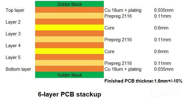
Stack-up represents the arrangement of layers in a PCB.It provides crucial information for PCB manufacturing,including the thickness of materials and copper foils required during production. Here is an example of a 6-layer stack-up structure with a total thickness of 1.6mm.

When designing a multilayer PCB,properly planning the stack-up structure is a crucial factor in ensuring optimal product performance.Improper board design and selection of unsuitable materials can lead to a decrease in the electrical performance of the signal transmission.It can also increase radiation and crosstalk,making the product more susceptible to external noise interference.These issues can result in timing failures and interference,ultimately causing intermittent operational problems and significantly impacting performance and long-term reliability.
Keep the power and ground layers together whenever possible,placing them adjacent to each other and as close as possible.The closer the distance between these layers,the larger the plane capacitance formed,which benefits power filtering.
Both the power and ground planes can serve as reference planes for signals,but it is recommended to prioritize the ground plane.
It is preferable to have a ground plane beneath the component side to provide a shielding layer for the components and serve as a reference plane for top-layer routing.
All signal layers should be adjacent to the ground plane as much as possible to ensure a proper current return path for signals.
Avoid directly adjacent signal layers whenever possible,and if unavoidable,try to keep the traces perpendicular.
Consider a symmetrical stack-up structure to avoid board warping issues.
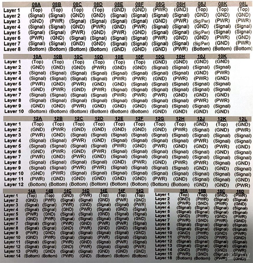
PCBWay manufactures multilayer circuit boards with layers in the range from 4 to 14 layers, board thickness from 0.4mm to 3.0mm, copper thickness from 1oz to 4oz, inner layer copper thickness from 1oz to 2oz, and minimal spacing between layers to 4mil. Following images present PCBWay's default layers stack-up of PCB service.
If you don't require customized PCB layer stack-up, we will make the multilayer PCBs according to our default layers stack-up as below.
