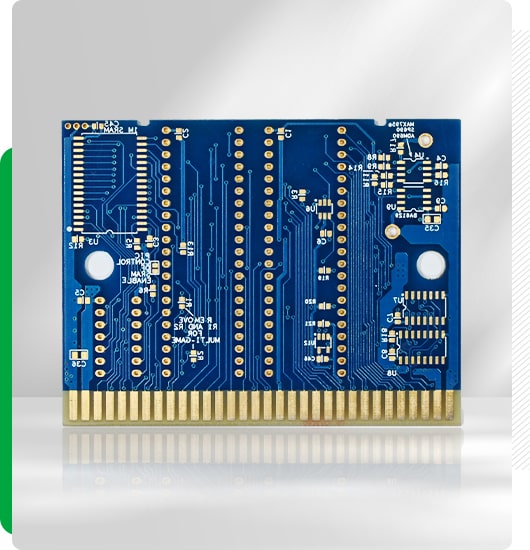
HDI PCB stands for High-Density Interconnect board. According to IPC-2226, HDI is defined as a printed circuit board with a wiring density per unit area higher than that of traditional printed circuit boards (PCBs). It is manufactured using micro-blind-buried via technology, resulting in high circuit distribution density. Therefore, HDI circuit boards are also referred to as buried blind via boards or blind and buried via circuit boards.

Microvias, with their smaller aspect ratio, provide enhanced reliability compared to typical vias. They are more robust and utilize superior materials and components, resulting in excellent performance in HDI (High-Density Interconnect) technology.
HDI technology employs via-in-pad, blind-via, and buried-via techniques, which bring components closer together, thereby reducing signal path lengths. By eliminating via stubs, HDI technology decreases signal reflection and improves signal quality, significantly enhancing overall signal integrity.
With proper planning, HDI technology can lower overall costs compared to standard PCBs. This is achieved through fewer layers, smaller dimensions, and a reduced number of required PCBs.
The use of blind and buried vias minimizes the space requirements of the circuit board.
| Feature | Capability |
|---|---|
| Via Types | Blind via, buried via, through-hole via |
| Number of layers | Up to 60 layers (evaluation required above 30 layers) |
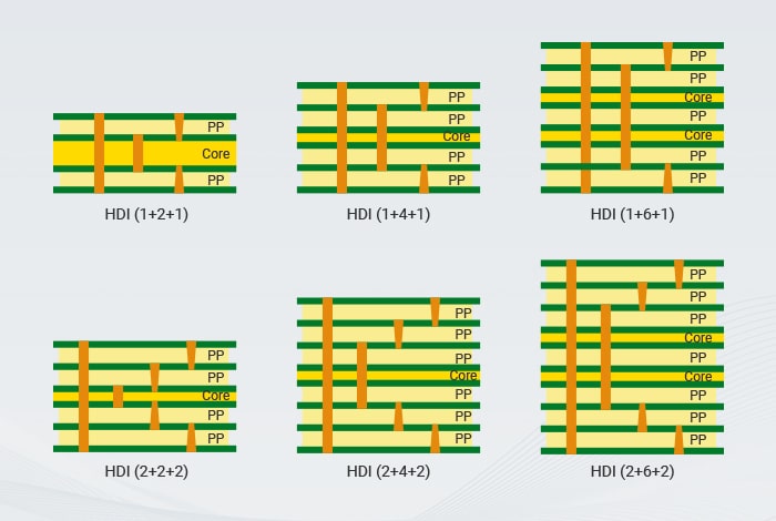
| HDI builds | 1+N+1, 2+N+2 , ... , 6+N+6(≥6 orders require evaluation) |
| Copper weights( finished) | 18um-70um |
| Min trace/spacing | 0.065mm/0.065mm |
| PCB thickness | 0.1-8.0mm (evaluation required for less than 0.2mm or greater than 6.5mm) |
| Max. PCB dimension(finished) | 2-20 layers, 21*33 inches; length ≤ 1000mm; evaluate if short side > 21 inches |
| Feature | Capability |
|---|---|
| Min. mechanical drilling | 0.15mm |
| Min. laser drilling | Standard 4 mil, 3 mil require evaluation (corresponding to single 106PP). |
| Max. laser drilling | 8 mil (corresponding dielectric thickness cannot exceed 0.15mm) |
| Min. controlled depth drilling | PTH: 0.15mm; NPTH: 0.25mm |
| Aspect ratio | Max 14:1; evaluate if greater. |
| Min. solder mask bridge |
4mil(green, ≤1OZ) 5mil(other colors, ≤1OZ) |
| Diameter range of resin-filled vias | 0.254-6.5mm |

Understanding different HDI PCB stack-up structures provides designers with greater flexibility in layer allocation, component placement, and routing options, enabling efficient utilization of available space and optimization of the PCB layout. The common HDI PCB stack-up structures are shown in the left diagram.
Get instant quoteAfter years of relentless R&D and technological advancement, PCBWay has become a benchmark in the rapid manufacturing of small to medium batch HDI PCBs. Evolving from the initial 1+N+1, 2+N+2 to 3+N+3, and now to 5+N+5/6+N+6/7+N+7, PCBWay has successfully transitioned from rapid prototyping to stable mass production, shaping a well-respected brand with a commitment to absolute quality assurance.


We offer transparent pricing, with no hidden fees. Our products are made in our own factories, so you can be sure of the quality.
In cases of higher circuit complexity, using structures with blind and buried vias often achieves better yield and lower costs, providing advantages over traditional through-hole designs.
The aspect ratio in a PCB refers to the ratio of the depth of a hole to its diameter. It is commonly used to assess the manufacturability and performance of the hole. A higher aspect ratio indicates that the depth of the hole is greater relative to its diameter, which can pose challenges in the drilling and filling processes.
PCBWay can perform laser drilling with a minimum of 4 mil and a maximum of 8 mil.
In standard prototyping, the minimum PP thickness for laser blind vias is 0.06mm.
In standard prototyping, the minimum core thickness for laser blind vias is 0.1mm.


